
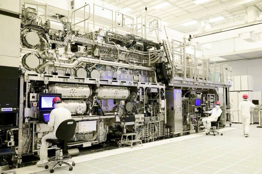
The global semiconductor industry has received one of its strongest signals yet that technological competition is entering a new phase. China has officially begun mass production of its own deep ultraviolet immersion lithography systems, equipment regarded as one of the most critical technologies in modern chip manufacturing. At London Hub Global, we believe the importance of this development extends far beyond the production of the first machines. It represents the creation of an independent technological foundation that could gradually reduce China’s reliance on foreign suppliers while reshaping the competitive balance across the global semiconductor industry.
The project is being coordinated by Shanghai Aishengna Electronic Technology Group, a state owned company established in August 2023 with registered capital of 7 billion yuan, equivalent to approximately $1 billion. Its shareholders include Shanghai Electric Holding and a subsidiary of Shanghai International Trust. Although the company has released virtually no public information about its operations, it has been entrusted with integrating the engineering capabilities of several of China’s leading lithography developers. We view this structure as evidence that Beijing is prioritizing a centralized industrial strategy rather than relying on individual startups, bringing together technology, financial resources and manufacturing capacity under a coordinated national framework.
According to available information, the project incorporates engineering teams from Shanghai Micro Electronics Equipment and the startup Yuliangsheng, which is affiliated with equipment manufacturer SiCarrier and supported by Huawei. This integration is expected to accelerate development across critical technologies, including optical systems, software, ultra precise mechanics and wafer positioning capabilities. At London Hub Global, we analyze this initiative as the logical continuation of China’s long term strategy to establish a fully independent semiconductor supply chain, covering everything from manufacturing equipment to large scale chip production.
Current production plans call for approximately five immersion DUV systems this year and around twenty units in 2027. Following additional testing, the first machines are expected to be delivered to major Chinese semiconductor manufacturers, including SMIC, Hua Hong Semiconductor and memory producer ChangXin Memory Technologies. Industry sources indicate that the new systems still trail ASML’s equipment in productivity, operational stability and technological maturity. As a result, they are not expected to replace Western lithography platforms in the near future. Even so, limited commercial deployment could significantly improve the resilience of China’s semiconductor industry if export restrictions become even more restrictive. We believe the key indicator will not be the number of machines produced, but rather how successfully they perform within commercial manufacturing environments.
Immersion DUV lithography remains one of the essential technologies behind today’s semiconductor industry. By introducing a thin layer of water between the projection lens and the silicon wafer, these systems achieve higher resolution than conventional dry lithography. They are widely used to manufacture processors, memory chips, automotive semiconductors and numerous industrial electronic components. Through multiple patterning techniques, DUV systems can also support more advanced manufacturing nodes, although this increases both production costs and manufacturing complexity. This explains why demand for high performance DUV equipment remains strong throughout the global semiconductor market.
The acceleration of domestic Chinese development is closely linked to international export restrictions. The United States has prohibited exports of ASML’s most advanced extreme ultraviolet lithography systems to China, while Dutch export controls have also restricted access to several of the company’s most advanced DUV platforms. In response, Beijing has significantly expanded investment in domestic alternatives. We emphasize that these restrictions create a dual effect. In the short term, they slow China’s technological progress, yet they simultaneously strengthen the economic and strategic rationale for developing independent domestic manufacturing capabilities.
Financial markets reacted immediately to reports that Chinese production had begun. Shares of ASML declined by more than 8 percent as investors reassessed the possibility that China could eventually establish an alternative supplier for the world’s largest semiconductor market. At present, however, most industry experts agree that no immediate commercial threat exists. ASML retains a substantial technological advantage built over decades of research and remains the world’s only manufacturer capable of producing commercial EUV lithography systems at scale.
For the United Kingdom and London, these developments carry important strategic implications. British investment funds remain among the largest participants in global technology markets, while London’s financial institutions maintain significant exposure to semiconductor companies across international equity markets. Any long term shift in the competitive balance between Western and Chinese equipment manufacturers could influence investment allocations, technology valuations and global supply chain strategies. The issue also reinforces the importance of technological security, which is becoming an increasingly central element of industrial policy across both Europe and the United Kingdom.
At London Hub Global, we view the launch of China’s domestic DUV manufacturing program as the beginning of a long term transformation whose significance will be determined not by today’s production volumes but by the pace of technological improvement over the coming years. If Chinese developers successfully demonstrate reliable commercial performance and gradually expand production capacity, the global lithography market is likely to become substantially more competitive. For investors, this reinforces the importance of monitoring not only semiconductor manufacturers but also equipment suppliers, export policy developments and government industrial strategies, as these factors are increasingly shaping the future architecture of the global semiconductor industry.